Place of Origin : Shenzhen,China
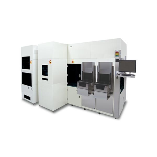
Automatic Wafer Cleaning Device After Light Resistance
Automatic Wafer Cleaning Device After Light Resistance
Product Description
Application Field: Removal Of Photoresistance/wafer Cleaning After Grinding
Wafer Size: 150mm&200mm&300mm (customizable)
Process Indicators: Wafers With Processes Above 19nm Can Be Cleaned
Automatic Wafer Plating Machine Features:
Equipped With 2 Or 3 Load Ports
Industrial Control Machine Touch Screen Operation Control, Convenient And Fast
Use Genuine Industrial Iot Configuration Software For Control And Monitoring
Support SECS/GEM Communication Protocol And Data Transmission
Horizontal Chamber, No Cross Contamination
Equipped With Two-arm Wafer Handling Manipulator Imported From Japan, Efficient And Stable
Equipped With Up To 8 Cleaning Chambers (customized)
Cleaning Liquid Independent Control, No Cross Contamination
Equipped With Nozzle Liquid Flow Accurate Control System
Our Products Are Very Popular, If You Are Interested In Our Products, Please Contact JuYongNeng As Soon As Possible.