Place of Origin :
Post Date : 26-10-2021
Expiry Date : 18-07-2024
In Order To Shorten The Signal Transmission Distance And Reduce The Signal Transmission Loss, The 5G Communication Board,Gradually Move Towards High-density Wiring, Fine Wire Spacing,The Development Of Small Aperture, Thin Profile And High Reliability.
Process Difficulty Of High Frequency And High Speed PCB Board
Alignment Accuracy
Accuracy Is Tightened, And Tolerance Convergence Between Layers Is Required. The Board Size Becomes More Demanding For This Convergence Requirement
Size Gets Bigger
Machinability Deteriorates, Maneuverability Deteriorates, And Blind Holes Need To Be Buried 1. Cost Increase 2. Difficulty In Alignment Accuracy
Impedance Accuracy
The Etching Challenge Is Great:
1. The Etching Factor: The Smaller The Better, The Etching Accuracy Tolerance Is 10mil And The Line Width Is Controlled By +/-1MIL, And The Line Width Tolerance Above 10mil Is Controlled By +/-10%.
2. Higher Requirements For Line Width, Line Spacing And Line Thickness. 3. Others: Wiring Density, Signal Layer Interference
STUB (Impedance Is Not Continuous)
STUB Is Tightened, Board Thickness Fluctuation Is Extremely Challenging, And Back Drilling Technology Is Required
Increased Signal Loss Demand
It Is A Big Challenge For All Copper Clad Laminates; The Tolerance Requirements For PCB Thickness Are High, Including Length, Width, Thickness, Perpendicularity, Bow And Twist, Etc.
The Number Of Layers Becomes Higher
Features Such As Denser Lines And Vias, Larger Cell Size, Thinner Dielectric Layer, Etc., More Stringent Requirements For Inner Layer Space, Interlayer Alignment, Impedance Control, And Reliability
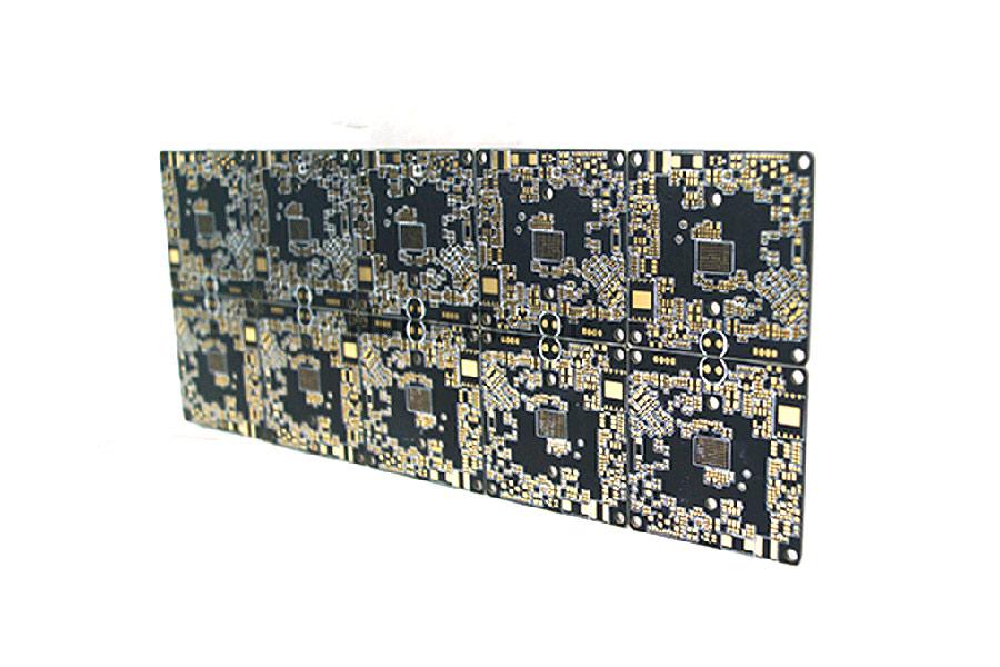
Accumulated Experience In Manufacturing Communication Board Of Huihe Circuits
High Density Requirements:
The Influence Of Crosstalk (noise) Will Decrease As The Line Width/spacing (L/S) Shrinks.
Strict Impedance Requirements:
Characteristic Impedance Matching Is The Most Basic Requirement For High-frequency Microwave Boards. The Greater The Impedance, The Greater The Ability To Prevent The Signal From Penetrating The Dielectric Layer, The Faster The Signal Transmission And The Smaller The Loss.
Transmission Line Production Accuracy Is High:
The Transmission Of High-frequency Signals Has Strict Requirements On The Characteristic Impedance Of The Printed Wire, That Is, The Production Accuracy Of The Transmission Line Is Generally ±lmil, And The Edges Of The Transmission Line Must Be Very Neat, And No Burrs, Gaps, Or Repairs Are Allowed. Line.
Mechanical Processing Requirements:
First, The High-frequency Microwave Board Material Is Very Different From The Epoxy Glass Cloth Material Of The Printed Board In Terms Of Machining; Secondly, The Processing Accuracy Of The High-frequency Microwave Board Is Higher Than That Of The Printed Board. Many, The General Shape Tolerance Is ±0.1mm (in The Case Of High Accuracy, The Shape Tolerance Is ±0.05mm).
Mixed Pressure:
The Mixed Use Of High-frequency Substrates (PTFE-based) And High-speed Substrates (PPE-based) Makes The High-frequency And High-speed Circuit Board Not Only Have A Large Conduction Area, But Also Have A Stable Dielectric Constant, High Dielectric Shielding Requirements, And High Temperature Resistance. At The Same Time, It Should Be Solved That The Differences In The Bonding Force And Thermal Expansion Coefficient Between The Two Different Plates Lead To The Undesirable Phenomenon Of Delamination And Mixed Pressure Warping During The Processing.
The Coating Uniformity Requirements Are High:
The Characteristic Impedance Of The High-frequency Microwave Board Transmission Line Directly Affects The Transmission Quality Of The Microwave Signal. The Characteristic Impedance Has A Certain Relationship With The Thickness Of The Copper Foil. Especially For Microwave Plates With Hole Metallization, The Plating Thickness Not Only Affects The Total Copper Foil Thickness, But Also Affects The Accuracy Of The Wire After Etching, So The Size And Uniformity Of The Plating Thickness Need To Be Strictly Controlled.
Laser Micro-Via Processing:
The Important Feature Of High-density Boards For Communication Is The Micro-via With Blind/buried Via Structure (aperture =0.15mm). The Formation Of Tiny Vias Is Currently Mainly Laser Processing. The Ratio Of The Diameter Of The Via Hole To The Diameter Of The Land May Vary From Supplier To Supplier. The Ratio Of The Diameter Of The Via Hole To The Connecting Plate Is Related To The Accuracy Of Drilling Positioning. The More Stacks, The Greater The Deviation May Be. At Present, The Target Positioning Is Tracked Layer By Layer. For High-density Wiring, There Have Been Vias Without Land.
Surface Treatment Is More Complicated:
As The Frequency Increases, The Choice Of Surface Treatment Becomes More And More Important; A Thin Coating With Good Electrical Conductivity Has The Least Impact On The Signal. The �roughness” Of The Wire Must Match The Transmission Thickness That The Transmission Signal Can Accept, Otherwise It Is Easy To Produce Serious Signal �s