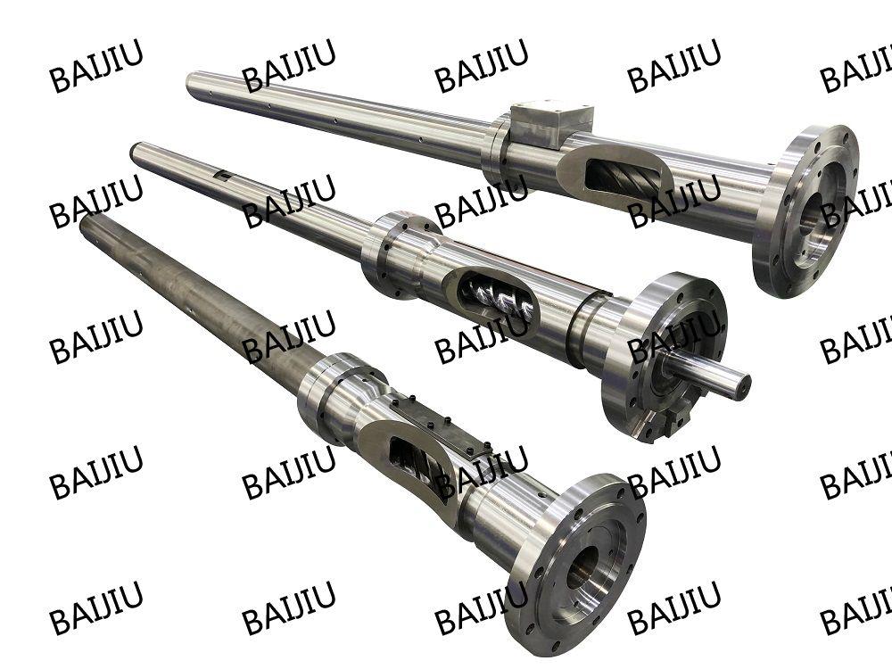
Place of Origin : Shenzhen,China
The plasma etch process is the removal of certain material from another substrate surface to leave a desired pattern. A mask helps prevent the material underneath from being etched. In general, the process in the plasma etching system involves ion bombardment to remove material. The process gas should be chosen so the rate of removal of the uncovered material is higher than the removal rate of the masking material. This process is generally used in the semiconductor industries.
The Plasma Etch Process Is The Removal Of Certain Material From Another Substrate Surface To Leave A Desired Pattern. A Mask Helps Prevent The Material Underneath From Being Etched. In General, The Process In The Plasma Etching System Involves Ion Bombardment To Remove Material. The Process Gas Should Be Chosen So The Rate Of Removal Of The Uncovered Material Is Higher Than The Removal Rate Of The Masking Material. This Process Is Generally Used In The Semiconductor Industries.
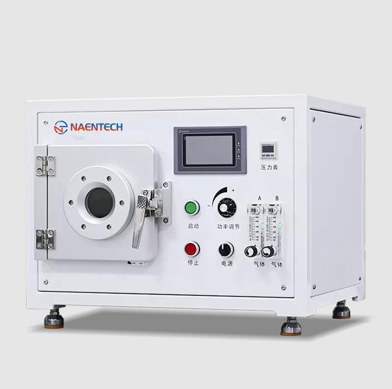
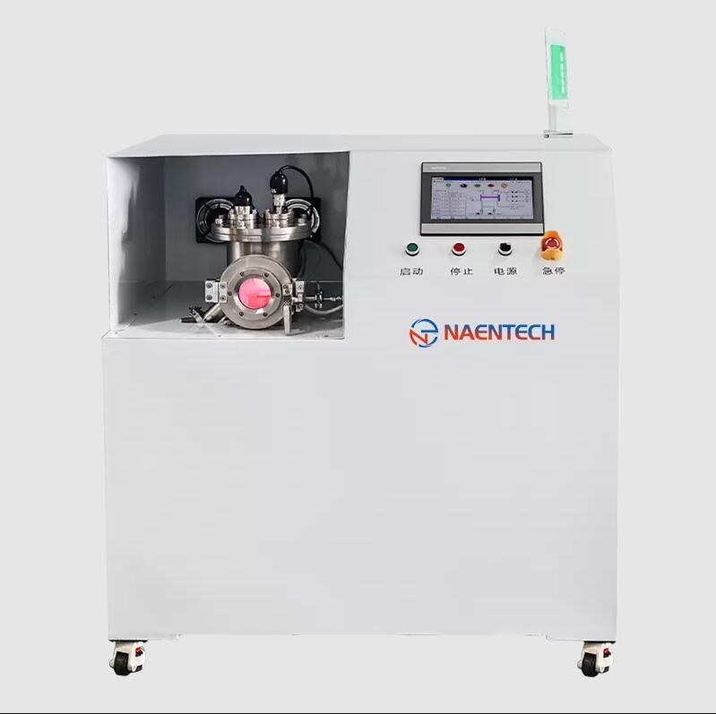
Plasma Etching Cleaner is A Reactive Ion Etching Device For Semiconductor Microfabrication Dry Etching. It Features A Compact Design, Simple Operation, And Excellent Process Repeatability. With The RIE Plasma Etching Mode, It Offers Fast Etching, High Uniformity, High Selectivity, And Strong Anisotropy.
Plasma Etching Systems Features:
RIE Mode For High-selectivity Anisotropic Etching, Meeting Strict Process Demands.
Full - Area Gas Showerhead And Axisymmetric Exhaust Ensure High Process Uniformity And Speed.
Heating And Lower Electrode Cooling Maintain Stable Etching Temperature, Rate, And Uniformity.
13.56MHz Solid - State RF Plasma Power With Auto Impedance Matching Guarantees Optimal Plasma Density And Repeatability.
Three Gas Channels With High - Precision Flow Meters Enable Flexible Process And Gas Selection.
Applications:
Etching Materials Like Si, SiO2, SiN, Poly-Si, GaAs, Mo, Pt, Polyimide, Etc.
Photoresist Ashing, Hydrophilic And Hydrophobic Modification, Surface Energy Enhancement, Introduction Of Functional Groups, Improvement Of Biocompatibility, Etc.